Outdated Drivers Are Slowing You Down
One free scan finds every outdated or missing driver and matches the right update for your exact hardware.Free scan · exact hardware matchWindows Errors? Fix Them Before They Spread
Repair common Windows errors and clear accumulated junk for a smoother, more stable PC - no reinstall needed.Free scan · no reinstallToner transfer is a practical way to make a simple copper-clad PCB at home: a laser printer deposits a fused-plastic pattern, heat and pressure bond that pattern to cleaned copper, and an etchant removes everything the toner does not cover. Reliable results depend less on maximum heat than on clean copper, suitable paper, even pressure, careful inspection and conservative trace geometry.
What toner transfer can—and cannot—do
The process is best for quick, single-sided prototypes and simple boards made with hand tools. It is not a guaranteed substitute for professionally manufactured PCBs: printer toner, paper, copper finish, board thickness and operator technique all affect the result. Fine lines, narrow clearances, dense packages and double-sided registration become progressively less forgiving.
As an Amazon Associate I earn from qualifying purchases.
Published trace limits are practical observations, not a universal specification. Dr. Lex reports that structures thinner than 0.17 mm can be troublesome in the described 300 dpi workflow, while Dr. Machine describes a method working down to about 0.3 mm for fast prototypes. Design with wider tracks and clearances than either figure where space permits, and verify your own printer-and-paper combination on a small test pattern.
Materials and equipment
- Blank copper-clad PCB laminate.
- A laser printer; inkjet ink is not the toner resist used by this method.
- Carrier paper intended for toner transfer, release-coated paper, or a glossy paper that you have tested. Paper performance varies considerably.
- A household iron with a controllable high-heat setting, or a laminator that can physically accept the board thickness.
- Fine abrasive pad, detergent or degreaser, lint-free cloth and clean water.
- Etchant suitable for your setup, a nonmetallic chemically compatible tray, plastic tweezers or tongs, gloves and splash-protective eye protection.
- Permanent resist marker for small repairs, solvent appropriate to the toner, and drill bits. A stable mini drill press is useful for repeated drilling.
Prepare artwork that transfers correctly
Mirror the copper layer
For a single-sided board, mirror the copper artwork before printing. Place the printed toner face against the copper; otherwise the finished board will be left-right reversed. Include board-edge references and small drill-center marks. Keep delicate features away from the edge and leave a trim margin.
#1 Best Overall
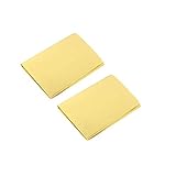
- A4 size layout, use a laser printer to put the PCB diagram on a smooth side, apply it to the copper plate, and put it into the rapid plate making machine or electric iron transfer.
- The production of printed circuit boards is often a headache for electronic enthusiasts. Many electronic enthusiasts often use amateur production methods such as paint tracing, knife engraving, and self-adhesive bonding to make a printed circuit board. It is slow and it is difficult to make high quality printed circuit boards.
- The production of printed circuit boards has become a "roadblock" for many beginners to enter the electronic hall. Therefore, DIY thermal transfer paper has become a must-have material for electronic enthusiasts to make high-precision circuit boards.
- The plate making process is low in cost, fast in speed and high in precision.
- Can make double panels.
Choose conservative geometry
A 300 dpi file can be adequate for the workflow described by Dr. Lex, who considers resolutions above 600 dpi unnecessary for that process. This is a practice note, not a manufacturing standard. Widen tracks, enlarge pads and increase spacing wherever your circuit allows. Avoid placing the finest artwork at an edge, where transfer pressure and heating are less uniform.
Print and test the carrier
Use a laser printer and a carrier with a known release surface. Specialty PCB toner-transfer paper may use a water-soluble dextrin barrier coating; PulsarProFX says its paper releases after immersion in water. Ordinary glossy papers can work, but the same paper may behave differently with another printer or toner. Run a small line-and-pad test before committing a full board, and keep the printer’s toner-density and media settings consistent once you find a workable combination.
Rank #2
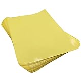
- Circuit Board Transfer Paper. Size: A4 / Color: Yellow / Quantity: 10
- Make sure you use the glossy side for transfer
- Make sure you use a laser printer
- Worked fine after I figured out the process
- laser printer PCB layout transfer paper
Clean the copper and transfer the toner
- Cut and prepare the blank. Cut the copper-clad board slightly oversize if you intend to trim it after etching.
- Abrade and degrease. Lightly abrade the copper until it is uniformly clean, wash away residue and oils, rinse and dry it completely. Do not touch the prepared surface with bare fingers.
- Align the print. Put the toner face-down on the copper and align the board outline, drill marks and any registration references. Tape the carrier only where it will not interfere with the transfer.
- Apply heat and pressure. With an iron, move methodically over the entire pattern so heat and pressure are even; the correct pressure takes practice. Insufficient heat or pressure leaves gaps, while excessive pressure can smear adjacent traces. A laminator can make the motion more repeatable only if the board fits safely through it.
- Soak and release. Let the assembly cool enough to handle, then immerse it in water. For release-coated specialty paper, the water dissolves the coating so the carrier can be peeled away. Remove paper gently rather than dragging it across the toner.
- Clear residue and inspect. Rinse away remaining coating, dry the board and inspect under magnification. Touch up isolated pinholes or missing spots with a permanent resist marker. If tracks have smeared together or large areas are missing, strip the toner and repeat instead of relying on an uncertain etch.
Etch safely and finish the board
Control the etch
Use an etchant appropriate to your equipment and follow its current label and safety data sheet. Ferric chloride is one commonly cited option; older guides also mention acid/peroxide systems, but chemical recipes and concentrations should not be copied as universal instructions. Use a nonmetallic, chemically compatible container, wear gloves and eye protection, prevent splashes and keep the work area ventilated as required by the product.
Do these 3 things before closing this tab:
1Repair Windows errors before they cause bigger problems2Scan for outdated or missing drivers - takes under a minute3Clear out junk files and repair common Windows errorsMonitor the board and remove it when exposed copper is gone. Leaving it in longer increases undercutting and can narrow traces. Rinse according to the etchant instructions, keeping the toner-covered copper protected until the etch is complete.
Rank #3

- 100PCS A4 Sheets Heat Toner Transfer Paper for DIY PCB Electronic Prototype Mak
Dispose of copper-bearing waste correctly
Do not pour spent copper-containing solution down a drain. Store and dispose of it according to local hazardous-waste rules and the selected chemical’s label or safety data sheet; requirements differ by jurisdiction.
Strip and drill
After rinsing and drying, remove the toner with a solvent approved for the product and use it as directed. Drill only after confirming your hole centers and trace clearances. Small HSS bits suit occasional holes; carbide bits cut cleanly for repeated PCB work but are brittle, so a stable drill press and careful handling reduce breakage.
Rank #4

- WHAT IS IT? - This tool provides a set of solder pads and jumpwire which can be used to re bridge wires on a circuit board as well as replace old, faded dots on a circuit board
- WHAT IS IT? - This tool provides a set of solder pads and jumpwire which can be used to re bridge wires on a circuit board as well as replace old, faded dots on a circuit board
- EFFICIENT - This jumpwire and pad set makes bridging and replacing old pads much easier than before making these types of repairs less hassle and increasing the efficiency.
- VARIETY - There are a variety of different jumpwire and pads in this set to help in multiple situations.
- APPLICATION - Either solder when bridging the wires or use green oil and UV to keep the pads in place on the board
Troubleshoot the transfer before etching
| Symptom | Likely contributors | Next adjustment |
|---|---|---|
| Toner has gaps or will not adhere | Greasy or oxidized copper, unsuitable paper, insufficient heat or pressure | Reclean the copper, test a different carrier, and change one heat or pressure variable at a time. Marker-touch small isolated defects. |
| Traces smear together | Excess pressure, excessive heat, or a printer/paper toner-density mismatch | Reduce pressure or heat slightly, review printer media settings and run a small test pattern. |
| Fine tracks break, especially near edges | Geometry too fine for the setup, uneven edge heating or undercut during etching | Widen tracks and clearances, move detail inward and leave a trim margin. |
| Double-sided artwork does not register | Insufficient alignment references or movement between transfers | Add matching fiducials and board-edge references; where practical, transfer and etch one side at a time while protecting the reverse side. |
Iron or laminator?
PulsarProFX says its process can be calibrated with a household iron and that a laminator makes use easier and faster. That is vendor guidance, not an independent comparison. An iron is inexpensive and accommodates unusual board shapes, but it relies on practiced, even movement. A laminator offers more repeatable passes when the board fits its feed path; never force a board through a machine that cannot accept its thickness.
How toner transfer compares with other home methods
| Method | Feature resolution | Equipment and setup | Process control | Chemical use |
|---|---|---|---|---|
| Toner transfer | Suitable for fast prototypes; practical limits vary with printer, paper and technique | Laser printer, carrier, heat source and drill tools | Requires tuning heat, pressure, release and etch time | Uses an etchant and produces copper-bearing waste |
| UV photoresist | Dr. Machine characterizes its described process as capable of finer features than toner transfer | UV exposure setup, resist-coated board and artwork alignment | Exposure and development must be controlled | Uses developer and an etchant |
| CNC isolation milling | Depends on fine tooling, machine rigidity and depth control | CNC router, suitable bits, fixturing and isolation software | Tool height and isolation depth are critical | Avoids chemical etching, though chips and dust still require control |
These are qualitative comparisons from Dr. Machine’s article, not standardized benchmark results. Choose toner transfer when low-cost, rapid, chemically manageable prototyping matters more than guaranteed fine geometry.
Best Value

- 【Material】 Material: FR-4 Glass Fiber, Copper; Layers: Double-sided.
- 【Size】Dimension: 150x100mm/ 5.91x3.94 inch(L*W); Thickness : approx. 1.5mm.
- 【Applications】Great for making PCB Circuit Board, Models. Widely used in product development, DIY experiments, maintenance, production, etc.
- 【Stable】Mechanically supports and electrically connects electronic components using conductive tracks, pads and other features etched from copper sheets laminated onto a non-conductive substrate.
- 【Note】The oxide layer on the surface of the copper-clad laminate needs to be polished clean with fine sandpaper to ensure that the carbon powder can be firmly printed on the copper-clad laminate during transfer. The surface of the board should be polished bright without obvious stains.
The Bottom Line
For dependable home-made boards, prioritize a spotless copper surface, mirrored laser artwork, a tested release paper, even heat and pressure, conservative trace dimensions, and a careful inspection before etching. Treat every quoted feature size as setup-specific, and handle etchant and copper waste as chemicals—not household rinse water.
Quick Recap
Product prices and availability are accurate as of the date/time indicated and are subject to change. Any price and availability information displayed on Amazon at the time of purchase will apply.